- 您现在的位置:买卖IC网 > Sheet目录472 > MAX2116EVKIT+ (Maxim Integrated)KIT EVAL FOR MAX2116
�� �
�
�Complete� DBS� Direct-Conversion� Tuner� ICs�
�with� Monolithic� VCOs�
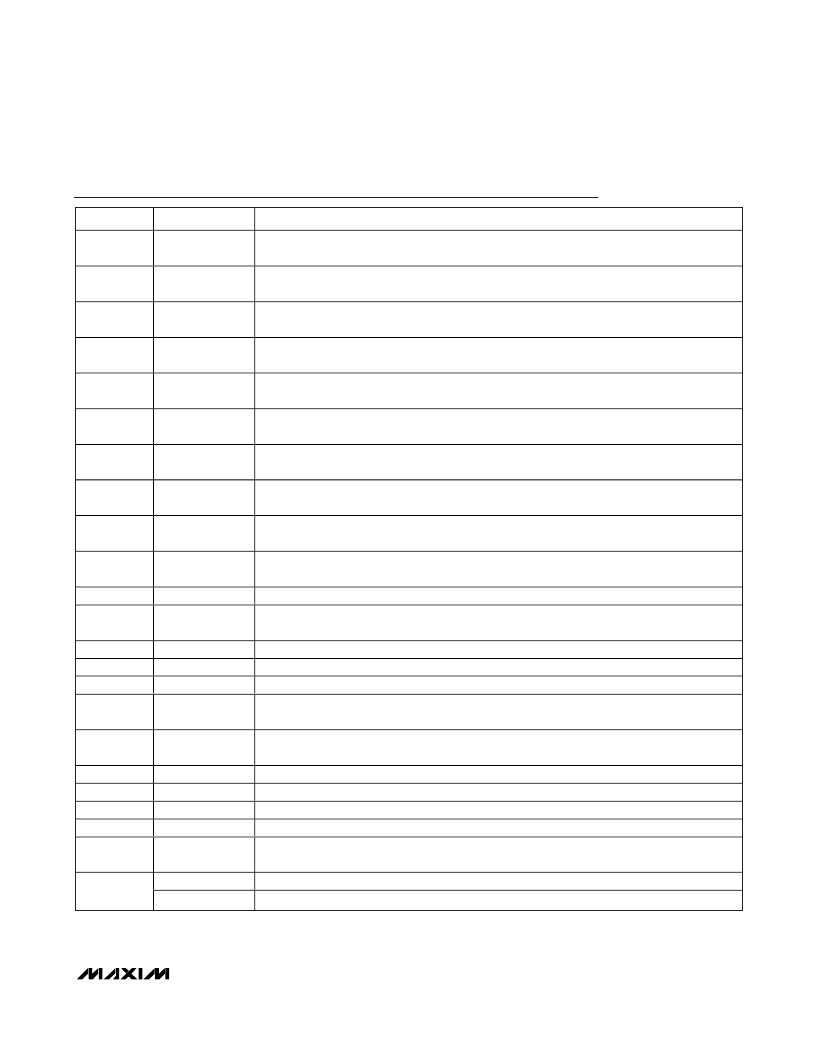
�Pin� Description�
�PIN�
�1,� 2�
�3�
�4�
�5�
�6,� 9,� 11,� 25,�
�31�
�7�
�8,� 28�
�10�
�12�
�13�
�14�
�15,� 26,� 32�
�16�
�17�
�18�
�19�
�20�
�21,� 22�
�23�
�24�
�27,� 29�
�30�
�NAME�
�IDC-,� IDC+�
�VCCRF1�
�RFIN-�
�RFIN+�
�N.C.�
�GC1�
�VREG1,� VREG2�
�PAD�
�VCCLO�
�VCCVCO�
�LOFLT�
�AS2,� AS1,� AS0�
�VTUNE�
�CPOUT�
�IFLT�
�VCCCPX�
�CFLT�
�XTL+,� XTAL-�
�CNTOUT�
�XTALOUT�
�SDA,� SCL�
�VCCDIG�
�FUNCTION�
�I-Channel� Baseband� DC� Offset� Correction.� Connect� a� 0.1μF� ceramic� chip� capacitor� from� IDC-�
�to� IDC+.�
�DC� Power� Supply� for� LNA� and� First-Stage� RF� VGA.� Connect� to� a� 5V� ±5%� low-noise� supply.�
�Bypass� with� a� 1nF� capacitor� directly� to� GND.� Do� not� share� vias.�
�75� Ω� RF-Inverting� Input.� Working� in� conjunction� with� RFIN+� for� differential� input.� Terminate� with�
�22pF� capacitor� in� series� with� a� 75� Ω� resistor� to� GND� for� single-ended� input.�
�75� Ω� RF� Noninverting� Input.� Working� in� conjunction� with� RFIN-� for� differential� input.� Connect� to�
�source� through� a� 22pF� series� capacitor.�
�No� Connection.� Pin� should� be� connected� directly� to� GND.�
�Gain� Control� Input� for� RF� Front� End.� High-impedance� analog� input� with� an� operating� range� of�
�0.75V� to� 2.6V.� VGC1� =� 0.75V� corresponds� to� maximum� gain.�
�2.85V� Linear� Regulator.� Used� for� terminating� open-drain� interfaces� from� demodulator.� Each�
�regulator� can� source� 3mA.�
�Ground.� Direct� connection� to� exposed� pad.� Can� be� used� to� check� exposed� pad� continuity� to�
�ground.�
�DC� Power� Supply� for� LO� Circuits.� Connect� to� a� 5V� ±5%� low-noise� supply.� Bypass� with� a� 1nF�
�capacitor� directly� to� GND.� Do� not� share� vias.�
�DC� Power� Supply� for� VCO� Circuits.� Connect� to� a� 5V� ±5%� low-noise� supply.� See� the�
�Applications� Information� section� for� more� details.�
�LO� Internal� Regulator� Bypass.� Bypass� with� a� 0.22μF� ceramic� chip� capacitor� to� GND.�
�I� 2� C� Address� Select� Control.� See� Table� 1� and� Table� 2.� These� pins� are� internally� pullup�
�to� V� CC� .� For� logic� high,� leave� these� pins� open.�
�High� Impedance� VCO� Tune� Input�
�Charge-Pump� Output�
�Test� Pin.� For� normal� operation,� connect� IFLT� to� ground.�
�DC� Power� Supply� for� Charge� Pump� and� XTAL� Oscillator� Circuits.� Connect� to� a� 5V� ±5%� low-�
�noise� supply.� Bypass� with� a� 1nF� capacitor� directly� to� GND.� Do� not� share� vias.�
�Bypass� for� Internal� Crystal� Oscillator� Bias.� Bypass� with� a� 0.22uF� ceramic� chip� capacitor� to�
�GND.�
�Crystal� Oscillator� Interface.� See� Typical� Operating� Circuit� .�
�Test� Pin.� Must� be� left� open.�
�Crystal� Oscillator� Buffer� Output.� Requires� a� 10nF� DC-blocking� capacitor.�
�I� 2� C� Data� and� Clock� Interface.� See� the� Applications� Information� section� for� details.�
�DC� Power� Supply� for� Digital� Circuits.� Connect� to� a� 5V� ±5%� low-noise� supply.� Bypass� with� a� 1nF�
�capacitor� directly� to� GND.� Do� not� share� vias.�
�33�
�N.C.� (MAX2116)� No� Connection.� Pin� should� be� connected� directly� to� GND.�
�QOUT-� (MAX2118)� Inverting� Baseband� Quadrature� Output�
�_______________________________________________________________________________________�
�9�
�发布紧急采购,3分钟左右您将得到回复。
相关PDF资料
MAX2117EVKIT+
KIT EVAL FOR MAX2117
MAX2120EVKIT+
KIT EVAL FOR MAX2120
MAX2121EVKIT#
KIT EVAL FOR MAX2121
MAX2130EVKIT
EVAL KIT MAX2130
MAX2140EVKIT
EVAL KIT MAX2140
MAX2150ETI+T
IC MODULATOR I/Q WIDE 28TQFN
MAX2160EVKIT
EVAL KIT MAX2160
MAX2163ETI/V+
IC TUNER ISDB-T LOW IF 28TQFN
相关代理商/技术参数
MAX2116UGL
功能描述:调谐器
RoHS:否 制造商:NXP Semiconductors 功能: 噪声系数: 工作电源电压: 最小工作温度: 最大工作温度:
MAX2116UGL-T
功能描述:调谐器
RoHS:否 制造商:NXP Semiconductors 功能: 噪声系数: 工作电源电压: 最小工作温度: 最大工作温度:
MAX2116UTL
功能描述:调谐器 RoHS:否 制造商:NXP Semiconductors 功能: 噪声系数: 工作电源电压: 最小工作温度: 最大工作温度:
MAX2116UTL+
功能描述:调谐器 Direct Conv Tuner w/Monolithic VCO RoHS:否 制造商:NXP Semiconductors 功能: 噪声系数: 工作电源电压: 最小工作温度: 最大工作温度:
MAX2116UTL+D
功能描述:调谐器
RoHS:否 制造商:NXP Semiconductors 功能: 噪声系数: 工作电源电压: 最小工作温度: 最大工作温度:
MAX2116UTL+T
功能描述:调谐器 Direct Conv Tuner w/Monolithic VCO RoHS:否 制造商:NXP Semiconductors 功能: 噪声系数: 工作电源电压: 最小工作温度: 最大工作温度:
MAX2116UTL+TD
功能描述:调谐器
RoHS:否 制造商:NXP Semiconductors 功能: 噪声系数: 工作电源电压: 最小工作温度: 最大工作温度:
MAX2116UTL+TG52
功能描述:调谐器
RoHS:否 制造商:NXP Semiconductors 功能: 噪声系数: 工作电源电压: 最小工作温度: 最大工作温度: